Simple AM Transmitter

There are not many AM transmitters that are easier to build than this one because the inductor is not tapped and has a single winding. There is no need to wind the inductor as it is a readily available RF choke (eg, Jaycar Cat LF-1536). To make the circuit as small as possible, the conventional tuning capacitor has been dispensed with and fixed 220pF capacitors used instead. To tune it to a particular frequency, reduce one or both of the 220pF capacitors to raise the frequency or add capacitance in parallel to lower the frequency. Q1 is biased with a 1MO resistor to give a high input impedance and this allows the use of a crystal ear piece as a low cost microphone.

Circuit diagram:
Author: Peter Goodwin

555 DC/DC Converter

It is all too often necessary to augment the power supply of an existing electronic circuit because exactly the voltage that you need is missing. The circuit presented here may provide a solution in a number of cases, since it can be used to convert a single-ended supply voltage into a balanced set of supply voltages. That’s not so remarkable by itself, but the special feature of this circuit is that this is accomplished without using difficult to obtain, exotic ICs. All of the components used in the circuit are ones that every electronics hobbyist is likely to have in a drawer somewhere.

The heart of the circuit is formed by an ‘old reliable’ 555 timer, which is wired here as a free-running oscillator with a frequency of approximately 160 kHz. The oscillator is followed by two voltage-doubling rectifiers, consisting of C1, D1, D2, C3 and C7, D3, D4, C5. They are followed in turn by two voltage regulators to stabilise the positive and negative voltages generated in this manner. The duty cycle of the 555 is set to approximately 50 percent using R1 and R2. The square-wave signal at the output of the timer IC has a DC offset, which is eliminated by C4 and R3.

555 DC/DC Converter
555 DC/DC Converter Circuit Diagram

The amplitude of the output signal from the 555 is approximately equal to the supply voltage less 1.5 V, so with a 12-V input voltage, there will be a square-wave signal on pin 3 with an amplitude of approximately 10.5 Vpp. With respect to ground (across R3), this is this +5 V / –5 V. Although this yields a symmetric voltage, its positive and negative amplitudes are somewhat too small and it is not stabilised. In order to split the square-wave signal into sufficiently large positive and negative amplitudes, C1/D2 are added for the positive voltage, causing the positive half to be doubled in amplitude.

For the negative half, the same effect is achieved using C7/D3. Following this, the two signals are smoothed by D1/C3 and D4/C5, respectively. Both voltages are now high enough to be input to normal 5-V voltage regulators, yielding symmetric +5V and –5V supply voltages at the output. The input voltage does not have to be regulated, although it must lie between +11 V and +18 V. The maximum output current is ±50 mA with an input voltage of 12 V. This circuit is an excellent choice for generating auxiliary voltages, such as supply voltages for low-power opamps. Naturally, the fact that the converter can be powered from the in-vehicle voltage of a car is a rather attractive feature.
Author: L. de Hoo - Copyright: Elektor Electronics

Touch-Select Audio Source

Often you need to connect output from more than one source (preamplifier) such as tape recorder/player and CD (compact disc) player to audio power amplifier. This needs disconnecting/connecting wires when you want to change the source, which is quite cumbersome and irritating. Here is a circuit that helps you choose between two stereo sources by simple touch of your hand. This circuit is so compact that it can be fixed within the audio power amplifier cabinet and can use the same power supply source. The circuit uses just two CMOS ICs and a few other componenets. The ICs used are MC14551/CD4551 (quad 2-channel analogue multiplexer) and CD4011 (quad 2-input NAND gate).
Touch-Select Audio Source

When touch-plate S1 is touched (its two plates are to be bridged using a fingertip), gate N1 output (IC1, pin 3) goes high while the output of gate N2 at pin 4 goes low. This causes selection of CD outputs being connected to the power amplifier input, which is indicated by lighting of LED1. When touch-plate S2 is touched, the outputs of gates N1 and N2 toggle. That is, IC2 pin 3 is pulled ‘low’ while its pin 4 goes ‘high’. This results in selection of tape recorder outputs being connected to the input of power amplifier. This is indicated by lighting of LED2. Pin 9 is the control pin of IC2.

In the circuit, the state of multiplexer switches is shown with pin 9 ‘high’ (CD source selected). When pin 9 is pulled ‘low’, all the switches within the multiplexer change over to the alternate position to select tape player as source. Note. Although one can connect pin 7 (VEE) of IC2 to ground, but for operation with preamplifier signals going above and below ground level, one must connect it to a negative voltage (say, –1V to –1.5V) to avoid distortion.

Motorcycle Battery Monitor

A circuit for monitoring the status of the battery and generator is undoubtedly a good idea for motorcyclists, as for other motorists. However, not every biker is willing to drill the necessary holes in the cockpit for the usual LED lamps, or to screw on an analogue accessory instrument.

The circuit shown here manages to do its job with a single 5-mm LED, which can indicate a total of six different conditions of the onboard electrical system. This is done using a dual LED that can be operated in pulsed or continuous mode (even in daylight). Built on a small piece of prototyping board and fitted in a mini-enclosure, the complete circuit can be tucked inside the headlamp housing or hidden underneath the tank.

Motorcycle Battery Monitor Circuit DiagramThe heart of the circuit is IC2, a dual comparator. The comparator circuit is built without using any feedback resistors, with the indication being stabilised by capacitors C4 and C5 instead of hysteresis. Small 10-µF tantalum capacitors work well here; 220-µF ‘standard’ electrolytic capacitors are only necessary with poorly regulated generators. Voltage regulator IC1 provides the reference voltage for IC2 via voltage divider R2/R3. The onboard voltage is compared with the reference voltage via voltage dividers R4 /R5 and R6/R7, which are connected to the inverting and non-inverting comparator sections, respectively.

Motorcycle Battery MonitorUsing separate dividers allows the threshold levels to be easily modified by adjusting the values of the lower resistors. IC2a drives the anode of the red diode of LED D4 via pull-up resistor R10. The anode of the green diode is driven by IC2b and R11. T2 pulls R11 to ground, thereby diverting the operating current of the green diode of the LED, if the voltage of the electrical system exceeds a threshold level of 15 V (provided by Zener diode D3). The paralleled gate outputs on pins 10 and 11 of IC3 perform a similar task. However, these gates have internal current limiting, so they can only divert a portion of the current from the red diode of the LED.

Table Power SupplyThe amount of current diverted depends on the battery voltage. The two gates are driven by an oscillator built around IC3a, which is enabled via voltage divider R14/R15 and transistor T1 when the battery voltage is sufficiently high. Depending on the state of IC3a, the red diode of the LED blinks or pulses. The circuit is connected to the electrical system via fuse F1 and a low-pass filter formed by L1 and C1.

If you cannot obtain a low-resistance choke, a 1-Ω resistor can be used instead. In this case, the values of C3, C4 and C5 should be increased some-what, in order to help stabilise the indication. D1 protects the circuit against negative voltage spikes, as well as offering protection against reverse-polarity connection. Due to its low current consumption (less than 30 mA), the circuit could be connected directly to the battery, but it is better to power it from the switched positive voltage.

NiCd Battery Charger

The design of the charger is similar to that of many commercially available chargers. The charger consists of a mains adaptor, two resistors and a light-emitting diode (LED). In practical use, this kind of charger is perfectly all right. Resistor R1 serves two functions: it establishes the correct charging current and it drops sufficient voltage to light the diode. This means that the LED lights only when a charging current flows into the battery. The charging current is about 1/4 of the battery capacity, which allows a slight overcharging, and yet the charging cycle is not too long (4–5 hours).
NiCd Battery Charger

The value of the resistors may be calculated as follows, for which the nominal e.m.f. and the capacity of the battery must be known. Adjust the output of the mains adaptor to 1.17 times the nominal battery voltage plus 3.3 V, which is the potential across R1. Note that the adaptor must be capable of supplying a current of not less than half the battery capacity. The value of R1 in ohms is equal to 3.3 divided by 1/4 of the battery capacity. The value of the resistors for various battery voltages is given in the Table. The battery capacity is taken as 1 Ah.
NiCd Battery Charger Circuit DiagramThe rating of R1 should be 5 W. If the battery to be charged has a different capacity, the theoretical value of R1 in the table must be divided by the battery capacity. Its actual value is the nearest one in the E12 series. For instance, if a 6 V battery with a nominal capacity of 600 mAh is to be charged, the value of R1 must be 20/0.6 = 33R.

LG G3 release date tipped for as early as May

Does it make sense for LG to launch the sequel to the LG G2 less than a full year after the flagship was announced? Probably not, but crazier things have happened in the mobile industry. Buzz out of Korea says LG could be targeting a May release (or at least announcement) for the LG G3, the name likely to be associated with the G2 successor.

Specifically, a date of May 17th is on the docket. Should we mark our calendars? History says not to hedge bets on rumored smartphone release dates so far in advance. Too much could happen between now and then to cause a shift in expected plans. That is, of course, assuming the report holds some shred of truth.

We agree it seems strange to launch a followup to the G2 in such close proximity to the the initial model’s release, but LG has the incentive to get a jump on the Samsung Galaxy S5. The Galaxy S5 looks to be the phone that the G3 will target as a direct competitor, and Samsung’s major smartphone announcement has typically occurred during the late spring/early summer (and looks to follow that pattern again this year).  If LG simply teases the phone or offers a full announcement while delaying actual commercial availability an additional month or two, it might be enough to steal some of Samsung’s thunder.

The report also reiterates specs that have previously been associated with the LG G3, including a 5.5-inch QHD display (2560 x 1440), LG Odin octa-core CPU, and 16MP camera. While these specs, like the release date, remain unconfirmed, they seem within the ballpark of reality. Still, take the whole thing with a but of skepticism.

Car Temperature Gauge

The Car Temperature Gauge is basically the same circuit as March's project with some minor changes to the input circuit. This circuit will display the water temperature to 1 degree resolution.

Car Temperature Gauge circuit diagram

Generation of 1-Sec Pulses Spaced 5-Sec Apart

This circuit using a dual-timer NE556 can produce 1Hz pulses spaced 5 seconds apart, either manually or automatically. IC NE556 comprises two independent NE555 timers in a single package. It is used to produce two separate pulses of different pulse widths, where one pulse initiates the activation of the second pulse. The first half of the NE556 is wired for 5-second pulse output. When slide switch S2 is in position ‘a’, the first timer is set for manual operation, i.e. by pressing switch S1 momentarily you can generate a single pulse of 5-second duration. When switch S2 is kept in ‘b’ position, i.e. pins 6 and 2 are shorted, timer 1 in NE556 triggers by itself.

The output of the first timer is connected to trigger pin 8 of second timer, which, in turn, is connected to a potential divider comprising resistors R4 and R5. Resistor R1, preset VR1, resistor R2, preset VR2, and capacitors C2 and C5 are the components determining time period. Presets VR1 and VR2 permit trimming of the 5-second and 1-second pulse width of respective sections. When switch S2 is in position ‘a’ and switch S1 is pressed momentarily, the output at pin 5 goes high for about 5 seconds. The trailing (falling) edge of this 5-second pulse is used to trigger the second timer via 0.1µF capacitor C6.
Generation of 1-Sec Pulses Spaced 5-Sec Apart

This action results in momentarily pulling down of pin 8 towards the ground potential, i.e. ‘low’. (Otherwise pin 8 is at 1/2 Vcc and triggers at/below 1/3 Vcc level.) When the second timer is triggered at the trailing edge of 5-second pulse, it generates a 1-second wide pulse. When switch S2 is on position ‘b’, switch S1 is disconnected, while pin 6 is connected to pin 2. When capacitor C is charged, it is discharged through pin 2 until it reaches 1/3Vcc potential, at which it is retriggered since trigger pin 6 is also connected here. Thus timer 1 is retriggered after every 5-second period (corresponding to 0.2Hz frequency). The second timer is triggered as before to produce a 1-second pulse in synchronism with the trailing edge of 5-second pulse.

This circuit is important wherever a pulse is needed at regular intervals; for instance, in ‘Versatile Digital Frequency Counter Cum Clock’ construction project published in EFY Oct. ’97, one may use this circuit in place of CD4060-based circuit. For the digital clock function, however, pin 8 and 12 are to be shorted after removal of 0.1µF capacitor and 10-kilo-ohm resistors R4 and R5.

Maximum Minimum Voltage Indicator

This circuit indicates which of three voltages in the range from about about -4V to about +4V - at A, B and C - is the highest by lighting one of three indicator LEDs. Alternatively, it can be wired to indicate the lowest of three voltages or to indicate both the highest and lowest voltages. Op amps IC1a, IC1b & IC1c are wired as comparators, while the three indicator LEDs and their series 1kO current limiting resistors are strung across the op amp outputs to implement the appropriate logic functions.

Circuit diagram:
Maximum minimum voltage indicator circuit schematic

For example, LED A will light only when pin 8 of IC1c is low (ie, A greater B) and pin 7 of IC1b is high (ie, A greater C). Similarly, LED B will light only when pin 8 of IC1c is high (ie, B greater A) and pin 1 of IC1a is low (ie, B greater C). LED C works in similar fashion if the voltage at C is the highest. Note that if all the LEDs and their parallel 1N4148 diodes are reversed, the circuit will indicate the lowest of the three input voltages. And if each 1N4148 diode is replaced by a LED, the circuit will indicate both the highest and lowest inputs.
Author: Andrew Partridge - Copyright: Silicon Chip

Video Amplifier

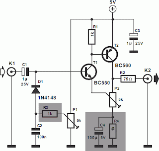
The video amplifier in the diagram is a well-known design. Simple, yet very useful, were it not for the ease with which the transistors can be damaged if the potentiometers (black level and signal amplitude) are in their extreme position. Fortunately, this can be obviated by the addition of two resistors. If in the diagram R3 and R4 were direct connections, as in the original design, and P1 were fully clockwise and P2 fully anticlockwise, such a large base current would flow through T1 that this transistor would give up the ghost.
Video Amplifier

Moreover, with the wiper of P2 at earth level, the base current of T2 would be dangerously high. Resistors R3 and R4 are sufficient protection against such mishaps, since they limit the base currents to a level of not more than 5 mA. Shunt capacitor C4 prevents R4 having an adverse effect on the amplification.

Solar Relay

With extended periods of bright sunshine and warm weather, even relatively large storage batteries in solar-power systems can become rather warm. Consequently, a circuit is usually connected in parallel with the storage battery to either connect a high-power shunt (in order to dissipate the excess solar power in the form of heat) or switch on a ventilation fan via a power FET, whenever the voltage rises above approximately 14.4 V. However, the latter option tends to oscillate, since switching on a powerful 12-V fan motor causes the voltage to drop below 14.4 V, causing the fan to be switched off.

In the absence of an external load, the battery voltage recovers quickly, the terminal voltage rises above 14.4 V again and the switching process starts once again, despite the built-in hysteresis. A solution to this problem is provided by the circuit shown here, which switches on the fan in response to the sweltering heat produced by the solar irradiation instead of an excessively high voltage at the battery terminals. Based on experience, the risk of battery overheating is only present in the summer between 2 and 6 pm. The intensity of the sunlight falling within the viewing angle of a suitably configured ‘sun probe’ is especially high precisely during this interval.

This is the operating principle of the solar relay. The trick to this apparently rather simple circuit consists of using a suitable combination of components. Instead of a power FET, it employs a special 12-V relay that can handle a large load in spite of its small size. This relay must have a coil resistance of at least 600 Ω, rather than the usual value of 100-200 Ω. This requirement can be met by several Schrack Components relays (available from, among others, Conrad Electronics). Here we have used the least expensive model, a type RYII 8-A printed circuit board relay. The light probe is connected in series with the relay. It consists of two BPW40 phototransistors wired in parallel.

Solar Relay Circuit Diagram

The type number refers to the 40-degree acceptance angle for incident light. In bright sunlight, the combined current generated by the two phototransistors is sufficient to cause the relay to engage, in this case without twitching. Every relay has a large hysteresis, so the fan connected via the a/b contacts will run for many minutes, or even until the probe no longer receives sufficient light. The NTC thermistor connected in series performs two functions. First, it compensates for changes in the resistance of the copper wire in the coil, which increases by approximately 4 percent for every 10 ºC increase in temperature, and second, it causes the relay to drop out earlier than it otherwise would (the relay only drops out at a coil voltage of 4 V).

Depending on the intended use, the 220-Ω resistance of the thermistor can be modified by connecting a 100-Ω resistor in series or a 470-Ω resistor in parallel. If the phototransistors are fastened with the axes of their incident-angle cones in parallel, the 40-degree incident angle corresponds to 2 pm with suitable solar orientation. If they are bent at a slight angle to each other, their incident angles overlap to cover a wider angle, such as 70 degrees. With the tested prototype circuit, the axes were oriented nearly parallel, and this fully met our demands. The automatic switch-off occurs quite abruptly, just like the switch-on, with no contact jitter.

This behaviour is also promoted by the NTC thermistor, since its temperature coefficient is opposite to that of the ‘PTC’ relay coil and approximately five times as large. This yields exactly the desired effect for energising and de-energising the relay: a large relay current for engagement and a small relay current for disengagement. Building the circuit is actually straightforward, but you must pay attention to one thing. The phototransistors resemble colourless LEDs, so there is a tendency to think that their ‘pinning’ is the same as that of LEDs, with the long lead being positive and the short lead negative. However, with the BPW40 the situation is exactly the opposite; the short lead is the collector lead. Naturally, the back-emf diode for the relay must also be connected with the right polarity. The residual current on cloudy days and at night is negligibly small.

Smoke Alarm Battery Life Extender

While smoke alarms are quite cheap devices, the cost of 9V batteries quickly exceeds their purchase price. Added to that is the irritation of random beeps from the alarm as the battery reaches the end of its useful life. This circuit allows typical smoke alarms to be powered from the 12V supply in a burglar alarm while still keeping the standard 9V batteries in place. It extends the 9V battery life to that of its "shelf life" as the battery is only required to drive the smoke alarm in the event the 12V supply is removed or shorted out.

Circuit diagram:
smoke alarm battery life extender circuit schematic
Smoke Alarm Battery Life Extender Circuit Diagram

In normal operation, the LM317 supplies 9.7V and this is fed via diode D2, resulting in just over 9V at the smoke alarm supply terminals. Q1 is not biased on, so the 9V battery is disconnected from the circuit. If the 12V supply is removed, the output of the LM317 will be 0V and Q1 will be biased on via the 4.7kO resistor and thus the smoke alarm will continue to be powered. The circuit could be assembled on a piece of Veroboard and fitted inside the smoke alarm. Alternatively, you could house the circuit and 9V battery within a standard electrical flush-mount box which the smoke alarm covers when mounted.
Author: Paul Blackler

Simple Battery Isolator

This circuit is even simpler and employs a 6V feed from one of the stator connections on the vehicle’s alternator. This is connected to a 6V automotive relay (RLY1) which controls a Continuous Duty Solenoid (RLY2). This solenoid electrically connects or isolates the batteries. When the engine is started and the alternator stator voltage rises, the 6V relay turns on. This turns on the Continuous Duty Solenoid to connect the two batteries in parallel. As long as the engine is running, the vehicle’s alternator will maintain charge in both batteries.

Circuit diagram:Simple Battery Isolator

When the engine is shut down, the alternator stator voltage drops and the Continuous Duty Solenoid switches off, thus isolating the second battery from the vehicle’s electrical system. Provided that camping accessories are only connected to the second battery, the main battery should never discharge. Because the concept is entirely dependent upon the alternator’s stator output voltage, you cannot forget to turn the system on or off as it happens automatically.

Cash Box Guard

Most thefts happen after midnight when people enter the second phase of sleep called 'paradoxical sleep.' Here is a smart security circuit for your cash box that thwarts the theft attempt by activating an emergency beeper. The circuit can also be used to trigger any external burglar alarm unit. The cash box guard circuit (shown in Fig. 1) is built around IC CD4060 (IC1), which has an inbuilt oscillator and divider. The basic oscillator is configured by a simple resistor-capacitor (R-C) network. IC CD4060 divides this oscillator frequency into binary divisions, which are available as outputs.

In light, reset pin 12 of IC1 remains low, which enables the oscillator built around IC1. However, in the dark, it making all the outputs low. This also stops oscillations of the internal oscillator. Working of the circuit is simple. If the cash box is closed, the interior will be dark. Hence in the dark, the light-dependant resistor (LDR1) resets IC1 and it stops oscillating and counting. At the same time, pins 13 and 14 of IC1 go low. So neither the piezobuzzer (PZ1) sounds, nor the relay (RL1) energises, indicating that the cash box is closed.

Cash Box Guard circuit diagram
Fig. 1: Cash box guard circuit

If someone tries to open the door of the cash box, light-most probably from the burglar's pen torch -falls on LDR1 fitted into the cash box. As a result, LDR1 conducts and pin 12 of IC1 goes low. IC1 starts oscillating and counting. With the present timing R-C components (at pins 9, 10 and 11), the output timing at pin 14 of IC1 is two-three seconds. Hence pin 14 of IC1 goes high for two seconds after the door is opened and goes low for another two seconds. So the piezobuzzer (PZ1) sounds for two seconds and then falls silent for the following two seconds. This cycle repeats until the cash box is closed.

An optional relay is added for a remotely located audio/visual alert system. For that, a relay driver circuit built around npn transistor BC548 (T2) is used. The relay is energised by the output from pin 13 of IC1 for about four seconds after the door is opened and then de-energised for the following four seconds. You can use this relay to activate another remotely located audio/visual alert system. After assembling the circuit on a small PCB, house it in a small tamper-proof box (refer Fig. 2) leaving a little window for LDR1 and a small opening for the piezobuzzer (PZ1). Now fit the unit inside the cash box (refer Fig. 3) with LDR1 pointing towards the door of the cash box.


Cash Box Guard
Fig. 2: Assemble unit

Note:
  1. The relay latching facility can be added to the circuit by replacing transistor T2 with a suitable silicon-controlled rectifier such as BT169.
  2. By changing the value of resistor R1, you can adjust the light detection sensitivity of the circuit.
  3. If you want to use a 3-pin piezobuzzer device, remove buzzer-driver npn transistor T1 and connect trigger pin of the buzzer directly to pin 14 of IC1. Also connect the positive and negative terminals of the buzzer to respective positive and negative points of the circuit.
  4. Photo-transistor 2N5777 can be used in place of the 10mm LDR1.

Cash Box Guard
Fig. 3: Unit fitted inside the cash box & also connected to an external alarm

HoneyDru USB Car Power Adapter

Having anything that is “cute” does seem to work these days, and considering how many of us carry a fair number of gadgets, it can be quite a task trying to make sure that all of them are fully juiced at the beginning of each day. Having said that, having a car charger in your ride is not too bad an idea after all, since you can never quite tell just when you might need to fall upon some backup power on the way to your meeting, with your smartphone running on empty. Why not get something cute while you are at it The $19.99 HoneyDru USB Car Power Adapter will certainly not disappoint, where this small, bee-shaped car power adapter will come with light-up eyes and wings for added “coolness” effect, especially during the evenings.
HoneyDru USB Car Power Adapter

Good thing nobody should be allergic to this bee-like USB car power adapter, as it does not sting at all, and the only thing it does well would be to power up those thirsty batteries in your well used gadgets. The HoneyDru USB Car Power Adapter would be plugged into most vehicles’ power outletcigarette lighter, and it is capable of 5V2A output, which should be more than some of the native chargers which accompany your devices. Apart from that, it will also feature a coiled cord which can be stretched to 3 feet and retracts to 8 inches for adaptability and flexibility .

Disposable Batteries Recharger helps stretch every last dollar


We do know that times can get pretty hard for some of us out there, especially when you are out of a job for the longest time and your savings have just about run out. Well, that would mean being even more prudent with every single penny that you spend, and there are many ways to do so. In the case of using disposable batteries, there might be a different method to prolong the life of these puppies even when others have long given up on them. How is that possible, you ask? Well, this is where the $79.95 Disposable Batteries Recharger comes in handy.

The Disposable Batteries Recharger happens to have enough storage space to revitalize up to eight disposable batteries simultaneously. The device itself will feature a sophisticated microprocessor and proprietary charging technology that will be able to automatically identify battery types as well as their conditions before the charging process begins. The unit itself will be able to recharge batteries in one to eight hours depending on the type and size, and it also has the ability to revitalize alkaline batteries up to 10 times. The eight charging slots has enough room to accommodate half a dozen AAA, AA, A, C, or D batteries and two 9-volt batteries, where it will play nice with alkaline, NiMH, or NiCd batteries. The inclusion of a built-in LCD will let you see the batteries’ charge levels. Man, I wish I had this back when I was a wee lad and was eating through AA batteries like nobody’s business on my Game Boy.

SDR Soundcard Tester

The key to using a soundcard successfully in digital signal processing or digital radio applications lies principally in the characteristics of the soundcard itself. This applies in particular to SDR (software defi ned radio) programs that turn your PC into a top-class AM/SSB/CW receiver, assuming your soundcard cooperates. If you want to experiment with SDR and avoid a lot of frustration, it is worth checking fi rst whether the PC soundcard you plan to use is suitable. There are three essential elements to success:
  • the soundcard must have a stereo line-level input;
  • the card must be equipped with an input anti-aliasing filter; and
  • the sample rate must be at least 48 kHz and the card must be able to cope with signals up to 24 kHz.
Many laptops have only a mono microphone input, sometimes also rather limited in bandwidth. In this case it may be possible to use an external USB soundcard. Most desktop PCs these days have an internal integrated soundcard, although some of these do not feature an anti-aliasing fi lter. Attempts to disable the integrated soundcard and replace it with a better one often meet with failure; again, an external USB soundcard is a possible solution.
SDR Soundcard Tester

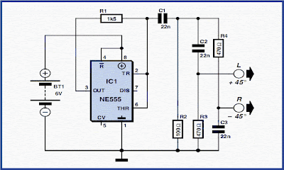
To avoid guesswork, the best way to proceed is to test the soundcard using this very small circuit. This will help to diagnose any problems and will help determine whether the card is suitable for use with an SDR program. Figure 1 shows a simple square-wave generator built around an NE555 timer IC. At the output is a 15 kHz signal rich in higher harmonics. Using this we can determine whether or not the soundcard can process the harmonics at 30 kHz, 45 kHz and so on. An anti-aliasing filter at the soundcard input should attenuate all signals above 24 kHz. The frequency of the test generator is, within limits, dependent on its supply voltage.

SDR Soundcard TesterUsing an adjustable power supply, a frequency range from 10 kHz to 20 kHz can therefore be covered. There are two RC networks at the output of the test circuit, a high-pass filter and a low-pass filter, acting as simple phase shifters. At the basic frequency of 15 kHz these provide a total phase difference of 90 degrees, corresponding exactly to the typical situation at the output of an SDR receiver circuit using an I-Q mixer: signals at the same frequency but differing in phase. To test the soundcard we need an SDR program running on the PC as well as the circuit of Figure 1. Suitable software includes SDradio (available for download from http://digilander.libero.it/i2phd/sdradio/).

When things are running correctly, the screen should display just two signals: the wanted signal at 15 kHz and a weaker image at –15 kHz (Figure 2). Suppression of the image may not be particularly good as the test circuit does not have very high phase and amplitude accuracy. If, however, the signals have the same level, there is a problem in the processing of the two channels: it is probable that the soundcard only has a monophonic input. If there is no anti-aliasing filter at the input of the soundcard the spectrum will show a large number of extra lines (Figure 3): it is easy to work out which harmonic corresponds to which alias frequency.

SDR Soundcard TesterThe results obtained using an I-Q receiver were grim: frequencies all the way out to 100 kHz were wrapped into the audible range, resulting in bubbling, hissing and whistling. In theory it would be possible to add an anti-aliasing filter to the output of the receiver to allow use with soundcards that are not equipped with such a filter. In practice, however, it is not easy to achieve the required sharp cutoff and symmetry between the two channels. A typical soundcard has a low pass filter set at 24 kHz which by 27 kHz is already attenuating the signal by some 60 dB. This is only practical using digital fi lters; an adjustable analogue circuit to achieve this performance would be so complex that the simplicity benefits of SDR receiver technology would entirely evaporate.
Author: Burkhard Kainka - Copyright: Elektor Electronics 2007

Stepped Volume Control

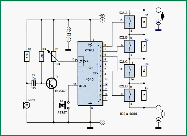
Louder music, sirens or speech in response to higher ambient noise levels? This simple circuit has the answer, and it may enable your robot to be at least as noisy or loud-mouthed as the others in an arena. The circuit consists basically of a microphone, a level detector, a 4-state counter and four analogue switches connected to a resistive ladder network. Looking at the circuit diagram, the signal from electret microphone M1 is amplified by T1 whose collector voltage appears across a potentiometer. M1 gets its bias voltage through R4. Depending on the setting of P1, the 4040 counter will get a clock pulse when a certain noise level (threshold) is exceeded.
Stepped Volume Control

The counter state determines the configuration of the four electronic switches inside the 4066 and so the series resistance effectively seen in the audio signal line. The circuit should be powered from a 9-V regulated supply or a battery and will consume a few milliamps only. Switch S1 allows the counter to be reset, switching all 4066 switches to off, i.e., the highest attenuation will exist in the audio path as in that case none of the 1-kΩ resistors are shorted out. To calibrate the circuit, disconnect the 4040 clock input (pin 10) from the wiper of P1, and temporarily ground it through a 100 kΩ resistor. Now pulse the clock input by briefly connecting it to the +9 V line; you will see the counter outputs change state and with them, the bilateral switches in the 4066.

Author: Raj K. Gorkhali Copyright: Elektor Electronics 2007

Low-Drop 5V Regulator

A 4-cell pack is a convenient, popular battery size. Alkaline manganese batteries are sold in retail stores in packs of four, which usually provide sufficient energy to keep battery replacement frequency at a reasonable level. Generating 5 V from four batteries is, however, a bit tricky. A fresh set of four batteries has a terminal voltage of 6.4 V, but at the end of their life, this voltage is down to 3.2 V. Therefore, the voltage needs to be stepped up or down, depending on the state of the batteries. A flyback topology with a costly, custom designed transformer could be used, but the circuit in the diagram gets around the problem by using a flying capacitor together with a second inductor.
Low-Drop 5V Regulator

The circuit also isolates the input from the output, allowing the output to go to 0 V during shutdown. The circuit can be divided conceptually into boost and buck sections. Inductor L1 and switch IC1 comprise the boost or step-up section, and inductor L2, diode D1 and capacitor C3 form the buck or step-down section. Capacitor C2 is charged to the input voltage, Vin, and acts as a level shift between the two sections. The switch toggles between ground and Vin+Vout , while the junction of L2, C2 and D1 toggles between –Vin and Vout +Vd1. Efficiency is directly related to the quality of the capacitors and inductors used.

Better quality capacitors are more expensive. Better quality inductors need not cost more, but normally take up more space. The Sanyo capacitors used in the prototype (C1–C3) specify a maximum ESR (effective series resistance) of 0.045 ½ and a maximum ripple current rating of 2.1 A. The inductors used specify a maximum DCR (direct current resistance) of 0.058 ½. Worst-case r.m.s. current through capacitor C2 occurs at minimum input voltage, that is, 400 mA at full load with an input voltage of 3 V.

Test Beeper For Your Stereo

The test beeper generates a sinusoidal signal with a frequency of 1,000 Hz, a common test frequency for audio amplifiers. It consists of a classical Wien-Bridge oscillator (also known as a Wien-Robinson oscillator). The network that determines the frequency consists here of a series connection of a resistor and capacitor (R1/C1) and a parallel connection (R2/C2), where the values of the resistors and capacitors are equal to each other. This network behaves, at the oscillator frequency (1 kHz in this case), as two pure resistors. The opamp (IC1) ensures that the attenuation of the network (3 times) is compensated for.

In principle a gain of 3 times should have been sufficient to sustain the oscillation, but that is in theory. Because of tolerances in the values, the amplification needs to be (automatically) adjusted. Instead of an intelligent amplitude controller we chose for a somewhat simpler solution. With P1, R3 and R4 you can adjust the gain to the point that oscillation takes place. The range of P1 (±10%) is large enough the cover the tolerance range. To sustain the oscillation, a gain of slightly more than 3 times is required, which would, however, cause the amplifier to clip (the ‘round-trip’ signal becomes increasingly larger, after all).
Test Beeper For Your Stereo

To prevent this from happening, a resistor in series with two anti-parallel diodes (D1 and D2) are connected in parallel with the feedback (P1 and R3). If the voltage increases to the point that the threshold voltage of the diodes is exceeded, then these will slowly start to conduct. The consequence of this is that the total resistance of the feedback is reduced and with that also the amplitude of the signal. So D1 and D2 provide a stabilizing function. The distortion of this simple oscillator, after adjustment of P1 and an output voltage of 100 mV (P2 to maximum) is around 0,1%. You can adjust the amplitude of the output signal with P2 as required for the application. The circuit is powered from a 9-V battery. Because of the low current consumption of only 2 mA the circuit will provide many hours of service.
Author: Ton Giesberts - Copyright: Elektor Electronics 2007

Dual Opamp Buffered Power Supply

There will be instances where the currents from each supply will be unequal. Where this is the case, the resistor divider is not sufficient, and the +ve and -ve voltages will be unequal. By using a cheap opamp (such as a uA741), a DC imbalance between supplies of up to about 15mA will not cause a problem. However, we can do better with a dual opamp (which will cost the same or less anyway), and increase the capability for up to about 30mA of difference between the two supplies.

Circuit diagram:Dual Opamp Buffered Power Supply
Dual Opamp Buffered Power Supply Circuit Diagram
Author: ESP

RS232 Voltage Regulator

There are many small applications where it would be preferable to power a device directly from an RS232 (V.24) interface, avoiding a mains power supply. Most ICs require 5 V, and the interface can provide a current of around 8 mA, almost all of which would be consumed by a readily-available voltage regulator, leaving nothing for the actual circuit. Using just four transistors we can construct a voltage regulator with current limiting which will allow us to draw more than the permitted 8 mA from an RS232 interface without damaging it. The example circuit in is configured for an output voltage of 5 V from an input voltage of at least 8 V, and a short-circuit current of 19 mA.

The current drawn by the regulator itself is only 0.2 mA. The circuit appears very simple, but it is more cunning than it looks. Few people appreciate what a handy device the transistor is. To meet the requirements for the circuit, the gains of the transistors need to be controlled carefully. Here only B-class devices are used, which have a gain of between about 220 and 280. Diodes D1 to D3 extract the positive voltage from the serial interface. Current limiting is achieved via resistor R1 and transistor T1. As soon as the voltage across the resistor reaches 0.7 V (at 18 mA with R1 = 39 Ω) the transistor turns on and thus turns off the output voltage by turning off T2. The output voltage of 5 V is set by Zener diode D4.

RS232 Voltage Regulator Circuit Diagram

Note that the output voltage is only approximate: beware when using components which have narrow supply voltage tolerances. When the Zener diode voltage and the voltage across transistor T4 are added together, the total is 5.8 V. However, because of T3, the diode is operating at a low current and the actual threshold for T4 is 4.9 V. The main regulation loop is built around R2 and T2. The high value of R2 (1.5 MΩ) is important, since this limits the maximum current through T2. At the output we would like to be able to draw a maximum current of 19 mA. The base of T2 must therefore be supplied with exactly 1/220 (the gain of the transistor) of 19 mA, and likewise the current into the base of T3 should be just 1/220 of 80 µA. With an input voltage of 9 V the voltage drop across R2 will be 3.3V, and so a current of 2.2 µA will flow. Transistor T3 multiplies this current by 220 to 0.5 mA, which is also the minimum quiescent current of the circuit.
Author: M. Müller
Copyright: Elektor Electronics

Hale Dreamer Alarm Clock Speaker Android Dock

Hale Dreamer Alarm Clock Speaker Android Dock tell you when it’s time to rise and shine
to sleep is not always as easy as laying down and shutting your eyes. For many, there is a bit of science to it. There needs to be little or no light, music or silence, and your phone either needs to be set to vibrate or have the volume turned down so you’re not woken up by every text. There is a nighttime mode that will screen calls for you, but there are docking systems out there that will cater to your specific needs a little bit better.
Hale Dreamer Alarm Clock Speaker Android Dock

The Hale Dreamer Alarm Clock Android Dock is a multi-function alarm clock that will give you the ability to do much more than just charge your phone. It has SmartSilence, which will silence your phone unless there’s an emergency, and it can act as a sound machine that has a optional shut-off timer with fade-out. In addition to giving you actual buttons to press, it plugs into your audio jack and micro USB to charge up your phone and play music through its 10w, full-range speakers.

There is a snooze button, as well as brightness and volume knobs. From this alarm clock, you’ll be able to set everything just the way you like it. You can choose how often you repeat your alarm, wake up to custom tones, the snooze length, and the numeral style. This will cost you around $80, which isn’t too bad for a docking system. The only thing it lacks is the light coming on gradually with your alarm. [Via]

Wall Mounted Bluetooth Speaker db60

Want a high quality audio that lets you enjoy those amazing music at home? Take a look at db60, the wall mounted Bluetooth speaker should be a nice solution. The db60 is a premium quality, award-winning Bluetooth wireless speaker that measures 268 x 195 x 160mm and weights 4.5kg.

Wall Mounted Bluetooth Speaker db60

As we can see from the images, the wireless speaker features sleek modern design, and comes with a specially designed shielded 4-inch Coaxial driver that is actually two drivers in one in order to produce high-quality room-filling audio for your favorite music. Moreover, the Bluetooth speaker also has an extra 3.5mm audio jack for other non-Bluetooth music players, and an built-in USB port allows to charge your smartphone just like a USB charger, while the integrated wing keeps your device in place when it’s charging do connecting with the wireless speaker.

Apart from that, its mount system allows you to easily mount the wireless speaker on the wall. At present the team of the db60 is raising fund at Kickstarter. Pledging £139 (approx $225) will let you own the wall-mounted Bluetooth speaker. If you’re interested, jump to Kickstarter official site for more details. [Via]

USB 5V to 12V DC-DC Step-Up Converter by LT1618

This is a 5V to 12V DC-DC step-up (boost) converter circuitry that is especially ideal for the USB powered applications. First of all a USB port has two current supply modes. Before detecting the connected device, it supplies maximum 100mA to the load. After recognizing the device, it increases the output current up to 500mA. In this circuit, controller (LT1618) also provides two input current modes. 100mA and 500mA input modes can be selected by the user.

USB 5V to 12V DC-DC Step-Up Converter by LT1618
Output currents are limited due to the increased potential difference at the output. When the demand of the load increases, output voltage will start to decrease. For example, if the circuit operates in the 100 mA input mode, when the load is 35 mA, the output voltage will be kept at 12V. But if the load increases to 50 mA,output voltage will reduce to 8V to maintain the constant 100 mA input current.

Negative-Output Switching Regulator

There are only a limited number of switching regulators designed to generate negative output voltages. In many cases, it’s thus necessary to use a switching regulator that was actually designed for a positive voltage in a modified circuit configuration that makes it suitable for generating a negative output voltage. The circuit shown in Figure 1 uses the familiar LM2575 step-down regulator from National Semiconductor (www.national.com). This circuit converts a positive-voltage step-down regulator into a negative-voltage step-up regulator. It converts an input voltage between –5 V and –12 V into a regulated –12-V output voltage.

Note that the output capacitor must be larger than in the standard circuit for a positive output voltage. The switched current through the storage choke is also somewhat higher. Some examples of suitable storage chokes for this circuit are the PE-53113 from Pulse (www.pulseeng.com) and the DO3308P-153 from Coilcraft (www.coilcraft.com). The LM2575-xx is available in versions for output voltages of 3.3V, 5 V, 12 V and 15 V, so various negative output voltages are also possible. However, you must pay attention to the input voltage of the regulator circuit. If the input voltage is more negative than –12 V (i.e., Vin < –12 V), the output voltage will not be regulated and will be lower than the desired –12 V.
Negative-Output Switching Regulator

The LM2575 IC will not be damaged by such operating conditions as long as its maximum rated input voltage of 40 V is not exceeded. High voltage (HV) types that can withstand up to 60 V are also available. Although the standard LM2575 application circuit includes circuit limiting, in this circuit the output current flows via the diode and choke if the output is shorted, so the circuit is not short-circuit proof.

 This can be remedied by using a Multifuse (PTC) or a normal fuse. There is also an adjustable version of the regulator with the type designation LM2575-ADJ (Figure 2). This version lacks the internal voltage divider of the fixed-voltage versions, so an external voltage divider must be connected to the feedback (FB) pin. The voltage divider must be dimensioned to produce a voltage of 1.23 V at the FB pin with the desired output voltage. The formula for calculating the output voltage is:

V out = 1.23 V × (1 + [R1 ÷ R2])

The electrolytic capacitors at the input and output must be rated for the voltages present at these locations.

Adjustable Symmetrical Power Supply Using LM317 and LM337

The circuit was designed to provide an adjustment with a power supply that is symmetrically designed while providing a voltage range of 1.25V to 30V at 1A current. LM317 – an adjustable 3-terminal positive voltage regulator capable of supplying in excess of 1.5A over an output voltage range of 1.2V to 37V and requires only two external resistors to set the output voltage due to its internal current limiting, thermal shutdown and safe area compensation, making it essentially blow-out proof LM337 – an adjustable 3-terminal positive voltage regulator capable of supplying in excess of 5A used as battery chargers, constant current regulators, and adjustable power supplies due to its features such as protected output from short circuit, product enhancement tested, current limit constant with temperature, guaranteed thermal regulation, adjustable output down to 1.2V, guaranteed 5A, and guaranteed 7A peak output current.

Adjustable Symmetrical Power Supply Using LM317 and LM337

The circuit will serve as a voltage converter with an input voltage of 35 V to produce an output voltage of 1.25 V to 30 V. The positive voltage is being handled by LM317 IC while the negative voltage is handled by LM337. The circuit can provide an output current of 1 A. During the production of 1 A current, the regulator is dissipating too much heat and without the presence of a heatsink, the regulator may get damaged.

Using these types of regulators provide features such as low noise and low price in the market. It can be made operational even with few components used. The only disadvantage that it will impose is the poor conversion efficiency. With the output of 35 V to 5 V, the efficient ratio of the output power with the input power is less than 42%. This is the reason why the switching regulator became cheap recently although the number of external components to be connected is minimally increased.

These regulators will work with better efficiency when used in case where current is more than 1A for more than 15 V and 0.4 A for less than 15 V from the power supply. Each regulator is adjusted for single positive and negative voltage output using the 10K ohms potentiometers RV1 & RV2. For dual outputs, a dual connected potentiometer RV3 is made to operate by switch S1. The visual indication on the voltmeter V1 is shown using the switch S2.
  • R1-2=270ohms
  • R3-4=2.2Kohms
  • R5-6=10Kohms
  • C1-5=100uF/63V
  • C2-4=100nF/100V
  • C3-8=10uF/25V
  • C6-10=100uF/63V
  • C7-9=100nF/100V
  • RV1-2=10Kohms Lin.
  • RV3=2X10Kohms Lin.
  • IC 1=LM 317T
  • IC 2=LM 337T
  • D1-2=1N4001
  • D3-4=1N4001
  • L1-2=LED 3mm
  • F1-2=1A slow Blow Fuse
  • S1-2=2X ON-ON SW
  • V1=0-30V DC Voltmeter
The adjustable symmetrical power supply is suitable to be used in audio amplifiers, microphone amplifiers, op-amp applications, impedance converters and other devices that require regulated positive and negative DC supply, since the output current is 1 A.

Switch-Mode Power Supply

National Semiconductor has been producing and designing ICs for use in switch-mode power supplies for many years. The application of these devices is normally straightforward, helped by the excellent documentation that is available. A typical example of a switch-mode power supply is that based on the LM2671 or LM2674. The components for it are available for outputs of 3.3 V, 5 V and 12 V. There is also a version providing a presettable output voltage. Within the specified application, the supplies can deliver currents of up to 500 mA. Note-worthy is the high switching frequency of 260 kHz.

Switch-Mode Power Supply

This has the advantage that only low-value inductor and capacitors are needed, and this results in excellent efficiency and small dimensions. In normal circumstances, the efficiency is 90% and may even go up to 96%. Both ICs provide protection against current and temperature overloads. The LM2671 has a number of additional facilities such as soft start and the option to work with an external clock. The latter enables several supplies to be synchronized so as to give better control of any EMC (ElectroMagnetic Compatibility). The application shown in the diagram provides an output voltage of 5 V and an output current of up to 500 mA. Diode D1 is a Schottky type  (Uco≥ 45 V and Imax≥ 3 A).

SSB Add-On For AM Receivers

Given favourable radio wave propagation, the shortwave and radio amateur band are chock-a-block with SSB (single-sideband) transmissions, which no matter what language they’re in, will fail to produce intelligible speech on an AM radio. SSB is transmitted without a carrier wave. To demodulate an SSB signal (i.e. turn it into intelligible speech) it is necessary to use a locally generated carrier at the receiver side. As most inexpensive SW/MW/LW portable radios (and quite a few more expensive general coverage receivers) still use plain old 455 kHz for the intermediate frequency (IF), adding SSB amounts to no more than allowing the radio’s IF to pick up a reasonably strong 455-kHz signal and let the existing AM demodulator do the work.

Circuit diagram:
SSB Add-On For AM Receivers


The system is called BFO for ‘beat frequency oscillator’. The heart of the circuit is a 455-kHz ceramic resonator or crystal, X1. The resonator is used in a CMOS oscillator circuit supplying an RF output level of 5 Vpp. which is radiated from a length of insulated hookup wire wrapped several times around the receiver. The degree of inductive coupling needed to obtain a good beat note will depend on the IF amplifier shielding and may be adjusted by varying the number of turns. All unused inputs of the 4069 IC must be grounded to prevent spurious oscillation. 
Author: D. Prabakaran - Copyright: Elektor 2004

Transformerless Power Supply

This circuit will supply up to about 20ma at 12 volts. It uses capacitive reactance instead of resistance; and it doesn't generate very much heat.The circuit draws about 30ma AC. Always use a fuse and/or a fusible resistor to be on the safe side. The values given are only a guide. There should be more than enough power available for timers, light operated switches, temperature controllers etc, provided that you use an optical isolator as your circuit's output device. (E.g. MOC 3010/3020) If a relay is unavoidable, use one with a mains voltage coil and switch the coil using the optical isolator.C1 should be of the 'suppressor type'; made to be connected directly across the incoming Mains Supply.

They are generally covered with the logos of several different Safety Standards Authorities. If you need more current, use a larger value capacitor; or put two in parallel; but be careful of what you are doing to the Watts. The low voltage 'AC' is supplied by ZD1 and ZD2. The bridge rectifier can be any of the small 'Round', 'In-line', or 'DIL' types; or you could use four separate diodes. If you want to, you can replace R2 and ZD3 with a 78 Series regulator. The full sized ones will work; but if space is tight, there are some small 100ma versions available in TO 92 type cases. They look like a BC 547. It is also worth noting that many small circuits will work with an unregulated supply.

Circuit diagram:Transformerless Power Supply Circuit Diagram

You can, of course, alter any or all of the Zenner diodes in order to produce a different output voltage. As for the mains voltage, the suggestion regarding the 110v version is just that, a suggestion. I haven't built it, so be prepared to experiment a little. I get a lot of emails asking if this power supply can be modified to provide currents of anything up to 50 amps. It cannot. The circuit was designed to provide a cheap compact power supply for Cmos logic circuits that require only a few milliamps. The logic circuits were then used to control mains equipment (fans, lights, heaters etc.) through an optically isolated triac.

If more than 20mA is required it is possible to increase C1 to 0.68uF or 1uF and thus obtain a current of up to about 40mA. But 'suppressor type' capacitors are relatively big and more expensive than regular capacitors; and increasing the current means that higher wattage resistors and zener diodes are required. If you try to produce more than about 40mA the circuit will no longer be cheap and compact, and it simply makes more sense to use a transformer. The Transformerless Power Supply Support Material provides a complete circuit description including all the calculations.

Web-masters Note:
I have had several requests for a power supply project without using a power supply. This can save the expense of buying a transformer, but presents potentially lethal voltages at the output terminals. Under no circumstances should a beginner attempt to build such a project.

Important Notice:
Electric Shock Hazard. In the UK,the neutral wire is connected to earth at the power station. If you touch the "Live" wire, then depending on how well earthed you are, you form a conductive path between Live and Neutral. DO NOT TOUCH the output of this power supply. Whilst the output of this circuit sits innocently at 12V with respect to (wrt) the other terminal, it is also 12V above earth potential. Should a component fail then either terminal will become a potential shock hazard.

MAINS ELECTRICITY IS VERY DANGEROUS.

If you are not experienced in dealing with it, then leave this project alone. Although Mains equipment can itself consume a lot of current, the circuits we build to control it, usually only require a few milliamps. Yet the low voltage power supply is frequently the largest part of the construction and a sizeable portion of the cost.

Negative Auxiliary Voltage

Some circuits need a negative supply voltage that only has to supply a small current. Providing a separate transformer winding for this (possibly even with a rectifier and filter capacitor) would be a rather extravagant solution. It can also be done using a few gates and several passive components. The combination of gate IC1a and the other three gates (wired in parallel) forms a square-wave generator. D1 and D2 convert the ac voltage into a dc voltage. As a CMOS IC is used here, the load on the negative output is limited to a few milliampères, depending on the positive supply voltage (see chart), despite the fact that three gates are connected in parallel.
Negative Auxiliary Voltage

However, as the figure shows, the negative voltage has almost the same magnitude as the positive input voltage, but with the opposite sign. If a clock signal in the range of 10–50 kHz is available, it can be connected to the input of IC1a, and R1 and C1 can then be omitted.

Negative Auxiliary Voltage circuit schematic
Author: Ludwig Libertin - Copyright: Elektor Electronics

Rugged PSU For Ham Radio Transceivers

This rugged power supply is based on the popular LM338 3-pin voltage regulator. The LM338 is capable of supplying 5 A over an output voltage range of 1.2 V to 32 V with all standard protections like overload, thermal shutdown, over-current, internal limit, etc., built in. In this power supply, some extra protections have been added to make it particularly suitable for use with low to medium-power portable and mobile VHF/UHF (ham) and 27 MHz transceivers. Diodes D4 and D5 provide a discharge path for capacitors C1 and C2. Diode D8 protects the supply against reverse polarity being applied to the output terminals. Capacitor C1 assists in RF decoupling and also increases the ripple rejection from 60 dB to about 86 dB.

If junction R1-R2 is not grounded by switch S1A, transistor T2 starts to conduct, causing the regulator to switch to zener diode D7 for its reference voltage (13 V). The PSU output voltage will then be 12.3 V. Normally, T2 will be off, however, and the PSU output voltage is then about 8.8 V. The high/low switch is useful to control the RF power level of modern VHF/UHF handhelds. Transistor T1, a p-n-p type BC557, acts as a blown-fuse sensor. When fuse F1 melts, T1 starts to conduct, causing LED D6 to light. If, for whatever reason, the PSU output voltage exceeds about 15 V, thyristor THR1 is triggered (typically in less than a microsecond).

Such a high-speed ‘crowbar’ may look like a drastic measure, but remember that this kind of protection is required by digital ICs that will not stand much overvoltage. The crowbar, when actuated, will faithfully destroy fuse F1 rather than allow the PSU to destroy expensive ICs. The two LEDs on the S1B contacts not only act as ‘high/low’ indicators but also as power-on indicators which are turned off when the mains voltage drops below about 160 V. If you envisage ‘heavy-duty’ use of the PSU, then voltage regulator IC1 should be mounted on as large a heatsink as you can get. The minimum we’d say is an SK129 heatsink from Fischer (Dau Components).

Input Impedance Booster II

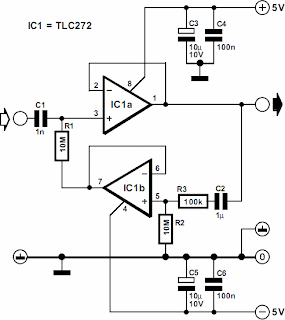
The input resistance of a.c.-coupled op amp circuits depends almost entirely on the resistance with which the d.c. setting is determined. If CMOS op amps are used, the input resistance is normally high, currently up to 10 MΩ. If a higher value is needed, a bootstrap circuit may be used. This enables the input resistance to be boosted artificially to a very high value, indeed In the circuit shown in the diagram, resistor R1 sets the d.c. point for IC1a. The terminal of the resistor linked to pin 7 of IC1 would normally be at earth potential, so that the input impedance would be 10 MΩ.

Input Impedance Booster II
Connecting the other terminal of the resistor to earth via IC1a and network C2-R3-R2 as far as d.c. is concerned results in the requisite d.c. setting of the op amp. As far as alternating voltages are concerned, the input signal is fed back so that only a tiny alternating current flows through R1. Therefore, Rin=R1[(R2+R3)/R3]. With resistor values as specified, Rin is about 1 GΩ. One aspect must be borne in mind: the numerical value of (R2+R3)/R3 must not exceed 0.99. This means that the value of R3 cannot be less than 100 kΩ if the value of R2 is 10 MΩ. If these conditions are not met, the circuit will become unstable.

Rechargeable Snow Blower

You know what they say –the grass is greener on the other side of the fence. How any people do you know wish that they stay in an area where snow is in abundance? For folks who happen to live in such an area, you know the hassle of life when it snows really hard, and nearly every single day during winter to boot. A snow blower would make plenty of sense actually, which is why you might want to check out the $599.95 Rechargeable Snow Blower.

Rechargeable Snow Blower

The Rechargeable Snow Blower is touted to be the only snow blower which will be powered by a rechargeable battery, hence doing away with the need to refill a gas tank, or perhaps to untangle a power cord. A 40-volt lithium-ion battery would run proceedings fro within, where this emission-free, environmentally friendly blower can throw powder for up to 40 minutes at a stretch before exhausting its battery reserves.

It works best in clearing out small outdoor spaces like a patio or walkway, where the single-stage blower is more than capable of handling 10″ high drifts and clear an 18″ wide path in a single pass. Want to do all of the snow clearing after dark? Not a problem, since the blower features a bright LED headlight that makes it a snap to do so even when the sun has gone down. [Via]

Luminescent Moon Clock

Have you ever gone to the great outdoors, where there is no light pollution at all to spoil the view of the night sky, allowing you to check out plenty of stars along the way? Of course, during a full moon, the entire orchestra of the cosmos looks even more stunning, and it surely brings a sense of awe and wonder to the world. If you were sitting out in the open field with your loved one, it is definitely worth snapping a photo of that romantic moment. However, with our current hectic lifestyles, finding a break is getting more and more difficult, so why not bring the moon to your room with the $49.95 Luminescent Moon Clock?
Luminescent Moon Clock

As the name of this timepiece suggests, this wall clock will glow in the night, sporting the face of the full moon. It will rely on the most recent glow-in-the-dark technology, allowing it to absorb enough energy during daylight hours so that it ends up giving out a soft, ethereal light in a darkened room for up to 4 hours each night. The lunar image itself has been printed to the back of the flat glass face so that there is no possibility of scratching happening. You will also be able to check out the broad impact basin of Mare Imbrium in the vicinity of 12-o’clock, the Sea of Tranquility at 3-o’clock, and the Tycho crater at 7-o’clock. Of course, for easier viewing of the time, even the clock’s hands will glow in the dark.

General-Purpose NiCd Battery Charger

There is a wide variety of NiCd (nickel-cadmium) battery chargers on the market, but there are not many that can work from an in car 12 V cigar lighter. Such a charger would, for instance, be of interest to campers and caravanners who do not have a 230 V a.c. mains supply available. To satisfy the needs of these users, a charger could be designed for operation from the cigar lighter, but it is, of course, of far greater interest if it could also work from the domestic mains supply. Furthermore, it would also be very useful if a number of cells, say, 1 to 4, of different format could be charged simultaneously.

Lastly, another benefit would be if the charger would automatically switch off once the battery or cells have been charged fully. The charger described in this article does all that: it accommodates batteries or cells Type R6 and R14. Switching off after a period of 2 h 30 m, 5 h, or 10 h is arranged by 3-way switch S1. The 2 h 30 m period is for charging Type R6 batteries (1/2 charge), the 5 h period for fully charging Type R6 batteries or half charging Type R14 batteries, and the 10 h period for fully charging Type R14 batteries. Light-emitting diode D1 lights when charging is taking place. Charging after the set period has elapsed can be continued, if so desired, only by switching the supply off and then on again.

The time periods are determined by counters IC1 and IC2, Type 4060 and 4020 respectively. The 4060 has an integral oscillator, whose frequency is set to 932 Hz with preset P1 and the aid of a frequency meter. For various reasons, such as the values of the components used and parasitic elements, the oscillator itself operates at a slightly higher frequency – of the order of 1 kHz. The frequency of the signal at the wiper of P1 is divided by 214, so that the frequency of the signal at Q13 of IC1 is 0.056 Hz, equivalent to a pulse every 17.6 s. The signal at Q13 is applied to the input, pin 10, of IC2. When switch S1 is in position 2 h 5 m (output Q10 of IC2), the divisor should be 210 (1024).

However, contrary to what these figures indicate, the time period stops at half that at output Q10. To obtain a charging period of 2 h 30 m, that is, 9,000 seconds, which should correspond to half a period at output Q9 of IC2, the oscillator period must be 9000×2/16.7×106=1.073 ms, which corresponds to a frequency of 932 Hz as mentioned earlier. On power-on, only counter IC2 is reset, since an error of a few seconds that may arise in IC1 is of no significance. This arrangement simplifies the design. When the time set has elapsed, that is, charging is finished, diode D1 goes out.

The charging current is fixed by darlington transistor T3, which is a classical design of a current source with negative feedback. The transistor tends to hold its emitter potential at 1.3 V, but this requires the aid of a zener diode, D2. In this type of design, the thermal stability is, in fact, totally acceptable, because the temperature of the zener diode, in view of the small current this draws and its consequent low temperature rise, hardly affects the charging current Transistor T1 is either on or off and serves to power the on/off indicator LED. It is needed to prevent an overload on the output of counter IC1 if this would be required to absorb the total current (about 7mA) drawn by the diode.

Transistor T2 discontinues the charging when the time set by S1 has elapsed by earthing the base of darlington T3. Diodes D3–D14 are connected in threesomes across the terminals of the batteries to be charged: D3–D5 across those of battery Bt1, D6–D8 across those of Bt2, and so on. Diode D15 prevents the batteries to be charged from being discharged when the supply fails. When the charger is used in a vehicle, additional precautions should be taken to ensure that any spurious surges on the vehicle power lines do not adversely affect the charger’ s operation. The battery holder should be one that can accommodate four size R6 (AM3; MN1500; SP/HP7; mignon) or R14 AM2; MN1400; SP/HP11; baby) batteries.

The length of these batteries, but not their diameter, is the same (about 45 mm). When the charger is used at home, it may be powered via a suitable 15V mains adaptor. It draws a current of about 150mA. A final word of warning: it is possible for batteries to be connected to the charger with incorrect polarity. This may result in a very large discharge current and even destruction of the battery. It is, therefore, imperative to verify the correct polarity of the battery before inserting it into the holder.

Remember Shelf

While we try our best, we can’t remember every small detail we’re supposed to keep track of. There’s gadgets to charge, groceries to buy, things to clean, appointments, meetings, and much, much more. While you can set reminders on your phone, that’s often not enough to make sure you accomplish whatever task lay in front of you in the appropriate amount of time. As the saying goes, “If you’re early, you’re on time. If you’re on time, you’re late.” Of course, if you’re late, it’s completely unacceptable.

The Remember Shelf will only work if you remember to use it

We need calendars that hang on the wall, notes on our hand, and post-its on everything. If all that isn’t enough, then the Remember Shelf can add to your collection. This is a a whiteboard where you can write down those appointment times and grocery list. It can also hold your keys, phone, and wallet. Possibly the most unique aspect of this is that there are switches on the right hand side where you can doodle little pictures of things that you still need to do.

That can be anything from turning off the light to locking the back door. It can become the best departure checklist for going out the front door before your day at work begins…well, if you remember to check it and update it regularly. This will cost you around $35, and won’t take up much space on the wall as it only measures 34x21cm. [Via]

Electronics Projects

Pulpit rock